8 Layer HDI PCB FR4 Material Blind And Buried Holes High TG170
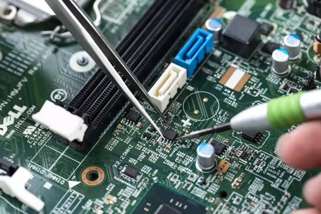
1 8 Layer HDI PCB with blind and buried holes.
2 Green solder mask and immersion gold treatment.
3 Min hole size is 0.1mm and min BGA size is 9mil.
4 Finished board thickness is 0.8mm.
5 The production cost will be higher than normal multilayer pcb and lead time will also be longer.
6 Need 3 round laminations and 4 round drillings.
7 2+N+2 hole structure: L1-L2 L2-L3 L1-L3 L7-L8 L6-L7 L6-L8 0.1MM, L3-L6 0.2MM, L1-L8 0.2MM.
8 ROHS, MSDS, SGS, UL, ISO9001&ISO14001 Certificated.
| Our Product Categories |
| Material Kinds | Layer Counts | Treatments |
| FR4 | Single Layer | HASL Lead Free |
| CEM-1 | 2 Layer/Double Layer | OSP |
| CEM-3 | 4 Layer | Immersion Gold/ENIG |
| Aluminum Substrate | 6 Layer | Hard Gold Plating |
| Iron Substrate | 8 Layer | Immersion Silver |
| PTFE | 10 Layer | Immersion Tin |
| PI Polymide | 12 Layer | Gold fingers |
| AL2O3 Ceramic Substrate | 14 Layer | Heavy copper up to 8OZ |
| Rogers, Isola high frequency materials | 16 Layer | Half plating holes |
| Halogen free | 18 Layer | HDI Laser drilling |
| Copper based | 20 Layer | Selective immersion gold |
| | 22 Layer | immersion gold +OSP |
| | 24 Layer | Resin filled in vias |
Q1: What is Surface Mount PCB Assembly?
A1: Surface mount in a PCB assembly means that each component on the PCB is mounted on the surface of the board. In the PCB Assembly process for surface mount components, solder paste is placed on the PCB board at areas where surface mount components will be placed on the board. PCB Stencils are usually used to apply solder paste on the PCB board and a pick and place machine is used to place SMT components on the board.
Surface Mount Assembly is very cost effective, takes up less board space and requires short production times as compared to thru-hole assembly, as it does not require the drilling of holes through the board. However, the component grip is not as good as thru-hole and also the connection can be faulty if not soldered properly.
Product Tags:

|
|
Blind Buried Holes Rapid Prototyping PCB 8 Layer HDI High TG170 FR4 Material Images
|


